- Get link
- X
- Other Apps
This post is created for personal use but i thought i might of some help for the others too.
Visit at this website elprocus.com for studying about the different sensors and modules.
Brain signals have voltage level of 10 micro volts.
48 billion gallons of water per people is available on earth, and 96% of that is available in ocean.
BJT as a switch
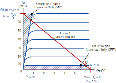
- Transistor switches can be used to switch and control lamps, relays or even motors.
- When using the bipolar transistor as a switch they must be either “fully-OFF” or “fully-ON”.
- Transistors that are fully “ON” are said to be in their Saturation region (Vbe=0.7v, Vbc ~= 0.5v, Vcesat=0.2v). In saturation region the formula Ic=Beta*Ib will no longer be available, and hence, Ic=BetaSat*Ib will be used.
- Transistors that are fully “OFF” are said to be in their Cut-off region(Vbe< 0.5v, Vbc < 0.4v and Ib=Ic=Ie=0).
- When using the transistor as a switch, a small Base current controls a much larger Collector load current.
- When using transistors to switch inductive loads such as relays and solenoids, a “Flywheel Diode” is used.
- When large currents or voltages need to be controlled, Darlington Transistors can be used.
BJT in Active region:
- BJT is said to be in active region, when Vbe = 0.7v, Vbc < 0.4v and Vce > 0.3v.
- In this mode Ic=Beta*Ib and Ie=(Beta+1)*Ib are applicable.
A capacitor charges to 63% of the supply voltage that is charging it after one time period. After 5 time periods, a capacitor charges up to over 99% of its supply voltage. Therefore, it is safe to say that the time it takes for a capacitor to charge up to the supply voltage is 5 time constants.
To calculate the time constant of a capacitor, the formula is τ=RC. This value yields the time (in seconds) that it takes a capacitor to charge to 63% of the voltage that is charging it up. After 5 time constants, the capacitor will charged to over 99% of the voltage that is supplying.
Therefore, the formula to calculate how long it takes a capacitor to charge to is:
Time for a Capacitor to Charge= 5RC
After 5 time constants, for all extensive purposes, the capacitor will be charged up to very close to the supply voltage. A capacitor never charges fully to the maximum voltage of its supply voltage, but it gets very close.
Example
Below we have a circuit of a 9-volt battery charging a 1000µF capacitor through a 3KΩ resistor:
One time constant, τ=RC=(3KΩ)(1000µF)=3 seconds. 5x3=15 seconds. So it takes the capacitor about 15 seconds to charge up to near 9 volts.
When a capacitor is fully charged no current flows through the capacitor.
Capacitors can be used to produce delay in the circuit.
This circuit is made to turn an LED on/off by using the a switch. R1 and C1 are introduced in the circuit to create the delay at ON/OFF time. Once the switch is pressed: Q1 will gets ON, once the C1 gets fully charged through R1 in R1C1 time. Remember no current will initially flows into the base of Q1 through R1 and R2. C1 gets fully charged and stops conducting then the current flows through R2 into the base of Q1 to make it turn ON.
When the switch is unpressed, the capacitor has charge to keep the circuit ON for R2C1 sec. and capacitor gets discharged. As a result, Q1 gets OFF after a delay.
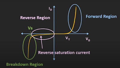
Working principle of Diode:
maximum forward bias allowable current
Reverse saturation current (Is)
forward bias threshold voltage (Vt)
breakdown voltage (till what voltage the diode can withstand in reverse bias)
Power dissipation
Reverse recovery time (how much time diode takes to go in reverse bias from the forward bias)
IN4148: reverse recovery time is 8nsec.
IN4007: reverse recovery time is 30usec.
PH4148: reverse recovery time is 4nsec.
Let say i am using a these diodes with a PWM of 16.67khz and varying duty cycle. Hence, period of PWM signal is 60usec. Because, the PWM is of varying width, therefore, IN4007 will not be able to switch properly because of its high reverse recovery time. But, IN4148 will work fine as it has low reverse recovery time.
Diode types:
- Rectifier diode
- Schottky diode
- zener diode
MOSTET testing:
This testing procedure is for use with a digital multimeter in the diode test-range with a minimum of 3.3 volt over d.u.t. (diode-under-test) Connect the 'Source' of the MosFet to the meter's negative (-) lead.
1) Hold the MosFet by the case or the tab but don't touch the metal parts of the test probes with any of the other MosFet's terminals until needed.
2) First, touch the meter positive lead onto the MosFet's 'Gate'.
3) Now move the positive probe to the 'Drain'. You should get a 'low' reading. The MosFet's internal capacitance on the gate has now been charged up by the meter and the device is 'turned-on'.
4) With the meter positive still connected to the drain, touch a finger between source and gate (and drain if you like, it does not matter at this stage). The gate will be discharged through your finger and the meter reading should go high, indicating a non-conductive device.
Such a simple test is not 100% -- but is useful and usually adequate.
When MOSFETS fail they often go short-circuit drain-to-gate. This can put the drain voltage back onto the gate where of course it feeds (via the gate resistors) into the drive circuitry, possibly blowing that section. It will also get to any other paralleled MosFet gates, blowing them also.
So, if the MosFets are deceased, check the drivers as well! This fact is probably the best reason for adding a source-gate zener diode; zeners fail short circuit and a properly connected zener can limit the damage in a failure! You can also add subminiature gate resistors -- which tend to fail open-circuit (like a fuse) under this overload, disconnecting the dud MosFet's gate.
What is break-before-make to avoid overlapping between the two changeover channels?
There are load switch ICs incorporating two switches. After the load switch IC “breaks” one switch, the break-before-make circuit keeps two switches off until it “makes” the other switch. This prevents two voltage domains from being short-circuited during the changeover between two switches.
Please also refer to the following documents for related explanations.
Propagation delay time (signal input to output) for CD4051BE at 5v is 60ns i.e it can operate at max of 16.66MHz. In case, you want lower delay from CD4051BE increase its operating voltage.
RTOS:
RTOS is recommended to use on a microcontroller having more than 4Kb of RAM.
follow to know more colin_walls@mentor.com
AT COMMANDS:
- AT+CMGR=1: read message at index 1
- Follow the link for more info on AT commands.
Whenever, we send commands to SIM900/800/908/808 etc. always wait for its response before sending another command.
Hence, it is always recommended to implement using CTS and RTS pins for hardware controlled flow of USART.
IC chips:
- AT89S52: processor
- V58JEY9K: Latch
- SIM900A, 900,808,800A, 800,800C, 908
- Link206, 306, 506
- ADM123: processor monitoring chip
- HCF4051: multiplexer
- MAX232: ttl to usb
- MAX112: ADC
- TLP701: gate driver ic
- LM317: can be used to make current source.
- ADM2483: RS485 transceiver.
- ADM1232: processor monitoring ic
- ATMELH236: EEPROM
- AT24C128: 128 kbit of Two wire I2C serial EEPROM
- ST24C02: 2kbit
- ST24C16: 16kbit
- ACS712:
24C16: 16 kbit=2 kbyte=2e11 byte hence this memory needs 11 bit of addressing. While working with these memories always use dedicated libraries.
1GHz, 64bit CPU: meaning this processor can push or receive data 1 billion times in a second, and everytime the data size is 64 bit. Therefore, it's bandwidth is 64 billion bits per second or 64 Gbps.
8bit, 12MHz: 12*10e6*8bits/sec is 96 Mbps.
APN: apn protocol connects the mobile network to the internet.
ASCII to decimal and decimal to ASCII conversation:
Let say we want to find out the ASCII value corresponding to decimal digit 0x03.
Just OR 0x03 with 0x30 and you will get 0x51 as ASCII value.
Now AND 0x51 with 0xCF and get 0x03 decimal again.
You need to remember only 0x30 and 0xCF.
surface mount technology: components size and their code.


Comments
Post a Comment