
We will first look at the digital to analog converter(DAC) circuit and then we will the analog to digital converter(ADC). This is because the ADC has D2C in its internal circuit and ADC depends on DAC for its operation.
DAC(really really fast as compared to the ADC): All the bits that are going to be converted in analog value, represented as a switch. If the bit is zero the corresponding switch will be OFF and ON for bit equal to 1. Depending upon the bits (state of the switches) there will be a voltage generated at the output of the opamp and that is nothing but the analog value corresponding to the bit represented digital value.
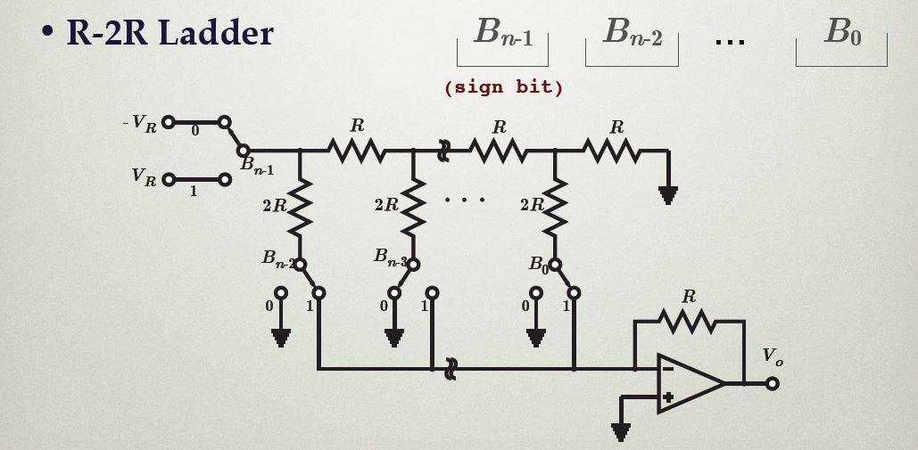 |
| DAC Circuit |
- The approximation circuit block contains the DAC.
- ADC uses two analog buffer to make sure that there is no loading problem and here analog buffer is made of opamp because it has very high input impedance.
- FET samples the analog value coming from the first analog buffer and charges the capacitor when the FET is ON to hold the value.
- Then the approx. circuit uses the voltage available in capacitor via an analog buffer.
- Digital buffer holds the bits while the next conversion is taking place in approx. circuit block.

Successive Approximation Analog to Digital Converter (Approx. Circuit Block):

- Vx is the voltage to be converted and Ain is the corresponding converted value. While, Vr is the reference value and it starts with Vr=0.
- If Vx>Vr then V0=+5 (why +5V?, because of logic level)
- if Vx<=Vr then V0=0
- SAL block updates the next bit in Ain to reflect V0.
- Vr is generated from the D/A convertion of Ain.
- Repeat this process from 2 to 10bits.

The above figure contains the plot of Vx vs time. Where, the dotted line represents the Vx= voltage to be converted into digital and red line indicates the reference voltage Vr.
- At t=t-minus,Vr=0V and Vx is at 3.39V and hence at t=t-plus, V0=+5V and V0 forms the first bit from MSB equal to 1.
- At t=t1-minus, Vr(generated from DAC)=(0+5)/2=2.5V and Vx=3.39V and hence at t=t-plus, V0=+5 meaning second bit from MSB equal to 1.
- At t=t2-minus, Vr=(2.5+5)/2=3.75V and Vx=3.39V and hence at t=t-plus, V0=0 and forms the thirst bit from MSB equal to 0.
- It keeps repeating the process by the number equal to the ADC-bit size.
- Each time the unknown interval is cut in half.
- For a 10bit ADC, This process repeats 10 number of times.
- Atmega328 takes 13clock cycle to convert a number, 10 clock cycles to form 10bits and then 3 clock cycles to manage and process those bits.
- Hence the Speed of ADC depends upon the clock we are using for ADC peripheral.
There is an alternative to this ADC and that is Quantization.

In quantization, we sample the signal at different time instant and look for its voltage and then assign a nearest digital voltage level shown on the vertical axis(This axis is divided in 5/2^10 levels for 10 bit ADC) to convert an analog data into digital. The blue dotted lines in figure represents the sampling time instant, red line shows the analog value to be converted, green line shows the digital level assigned to the samples values.
ADC of Atmega328:
- There are 6 channels, multiplexed and single ended with an accuracy of plus-minus 2LSB
- Takes 13 clock cycles to convert an analog value into digital.
- Input voltage range from 0-Vcc.
 |
| Complete ADC Block for Atmega328 |
With the help of ADMUX register Mux decoder selects the one channel at a time.
Looking closely on the figure

What are sources for ADC, 6-ADC channels from ADC0 to ADC5 (Remeber ADC6 and ADC7 are not available in Atmega328 chip), bandgap reference, temperature sensor.
Once a channel is selected by the mux decoder block, it goes to the comparator. as shown in the below figure

When we are using 5V reference(AVCC) then the resolution may not be good for your project and hence atmega328 offers a low reference voltage at pin AREF(user will input this voltage externally) to improve the resolution, and there is one more internal reference of 1.1V that gives really a better result.
So there are three voltage references 5V, 1.1V and AREF(user defined). We can use them by keeping in mind that whatever the reference voltage has been chosen the input analog voltage should be in that range. For the case 1.1V reference is chosen then the input analog voltage of 0-1.1V will cover the entire range 0-1024 and any value beyond 1.1V will result in full scale reading of 1024 and this voltage beyond 1.1V should not exceed 5V else it will damage the ADC.
Basic and essential registers to control the ADC are given in the figure below.

There are three essential register to work with the ADC and that are...
- ADC Multiplexer select (ADMUX)
- ADC CTRL and Status register (ADCSRA)
- ADC Data register (ADCH/ADCL)
ADMUX:

01: AVCC with external capacitor at AREF pin is by default in arduino.


ADC Operating Modes:
- Single conversion mode (on demand)
- Free running mode (continuously)
- Clocked conversion (periodically, requires ISR)
ADCSRA:

ADEN: ADC enable
ADSC: ADC start conversion
ADATE: ADC auto trigger enable, required for on demand and continuously mode
ADIF: ADC interrupt flag
ADIE: ADC enable
ADPSx: ADC clock prescalar bit, clock divisor: 2^n, n=[bbb]
ADCSRB:
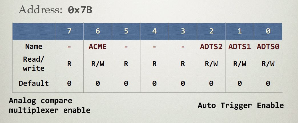
ACME: analog compare multiplexer enable bit enables us to use the analog comparator present in the arduino uno development board chip ATmega328.

DIDR0: If you are going to use the analog input to the Pin A0-5, then for proper functioning of ADC, first you need to make sure that the digital inputs to that pins are disabled. And this digital disabling on Pin A0-5 is assured by using the register DIDR0. Actually there is a buffer attached to the Pin A0-5 for the case when you want to use these pins for digital I/O and hence, its our compulsion to disable them whenever we want to use them as analog I/O.

ACSR: Analog comparator control and status register

DIDR1: Digital input disable register 1
In case we want to use digital comparator, then we need to disable the digital buffer connected to those pins before using them. This disabling is achieved by using the register DIDR1.

Free Running "Auto-trigger" mode:
- Can be clocked or unclocked.
- When clocked, an ISR is required.
- Clocked or not, the ADC performs one conversion after another.
- This can be an energy hog. Because doing ADC conversion continuously consumes power.
Let say i want to continuously convert analog input channels AIN3
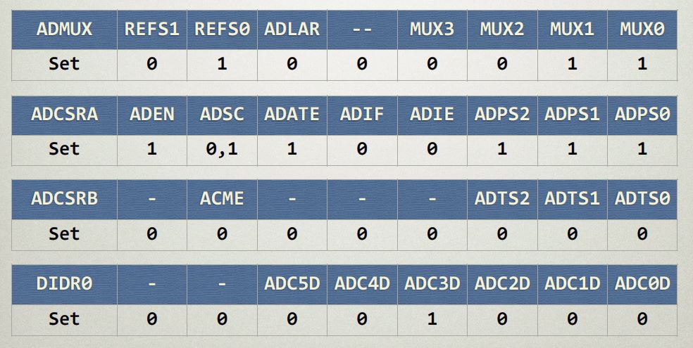
The setting in ADMUX, ADCSRA, ADCSRB, and DIRDR0 will be set as follows
In Atmega328, ADC gives very good accuracy at the sampling frequency less than 200KHz and hence the prescalar ADPS0:2 are selected to 111. Dividing 16MHz(div it by 13cycles/conversion gives us the max sampling frequency and that is about 1.23 MHz) by prescalar 2^7=128 gives us 125KHz.
ADSC: bit has 0,1 because this bit is needed to be toggled to start the conversion.
CODE:
- void setup(){
- ADMUX = 0b01000011;
- ADCSRA = 0b10100111;//here ADSC is zero
- ADCSRB = 0bx00;
- DIDR0 = 0b00001000;
- SDCSRA |= 0b01000000;//start conversion;//here ADSC is setting to 1
- }
- void loop(){
- int highbyte, lowbyte,value;
- highbyte = ADCH;//ADCH contains two MSBs out of 10bits.
- lowbyte = ADCL;//ADCL contains 8 remaining lower bits out of 10bits.
- value = (highbyte<<8)|lowbyte;
- }
NOTE: When we do the reading we have to read the higher byte first and then lower byte because reading the lower byte clears the variable values ADCH, ADCL. Hence it is necessary to take care while reading the values from these two variables. First read higher byte and then lower byte.
This blog is open to suggestions, please do leave a comment below.....
Click Next to study about Interrupts in Atmeaga328 microcontroller.
Comments
Post a Comment