L6....
Arduino pin diagram:


- IOREF
- AREF
- VIN
- input voltage to the Arduino UNO board when it is running from the external power.


- Watchdog Timer: is used to wake the system up by means of watchdog oscillator. Watchdog timer can also be used to reset the processor in case processor is met certain condition.
- Timer/Counter: are just the pulse counter to keep track of timing.
- TWI or I2C
Feature of Atmega328

- Instruction set are reduced as compared to the complex instruction set computer(CISC) i.e. x86
- Simpler intructions execute faster
- Other RISC machine: ARM, PowerPC, and SPARC
- Became popular in 1990s
Processor Layout

AVR Registers
- There are 32, 8bit registers mapped to address 0-32 in data space
- Most instruction can access any register and complete in one cycle
- Last 3-register pairs can be used as 3, 16bit index registers
- stack pointer size is 32 bit.
Flash Memory
- non-volatile
- 16-bit width
- some device have separate lockable boot section, meaning that once the code is written to the flash, it will not be read from the flash back to the PC, this is to improve the flash code security.
- at least 10000 write/erase cycles
SRAM

- we can add external SRAM if needed
- we are using 2048x8 byte of flash in case of atmega328
EEPROM
- non-volatile
- 8 bit width
- requires special write sequence
- at least 100000 write/erase cycles
ALU
- directly connected to all 32 general purpose registers
- operation between registers(only) executed within a single clock cycle
- support arithmetic, logic and bit functions
- on-chip 2-cycle multiplier and there is no divider but divider can be implemented using modulo
131 instructions
- Arithmetic & logic
- branch
- bit set/clear/test
- data transfer
- MCU control
Instruction Timing
- Register to Register---------1 cycle
- Register to Memory---------2 cycles
- Branch instruction-----------1-2 cycles
- Subroutine call & return-----3-5 cycles
- Some operations may take longer when dealing with external memory
AVR clock systems
- Clock control module generates clocks for memory and IO devices
- Multiple internal clock sources are available
- There is a provision for external clock source, is available. It can be max of 20MHz and on Arduino UNO board there is a clock source of 16MHz external to the Atmega328 micro-controller.
- Default is internal RC-8MHz oscillator prescaled by 8, yeilding 1 MHz CPU clock
- Default is only 5-10% that is far less than the external one's accuracy.

There are 5 clock sources to the AVR, 4 sources are for the AVR peripherals except the Timer/counter peripheral and one among 4 possible sources can be chosen using the clock mux. Timer/Counter oscillator is reserved for the timer/counter peripheral.
All the peripherals rely on the synchronous clock source.
Power Management
- Multiple power down modes
- wake on external reset or watchdog reset
- Power save mode
- wake on timer events
- several standby modes
- Unused modules can be shut-down
Reset Sources
- Power on reset
- External reset
- watchdog system reset
- Brown out detect(BOD) reset : when the voltage to the processor falls below a certain level that the processor can not function reliably, then the condition is called as Brown out detect and in this condition the processor can be reset by means of code.
Interrupts
- Atmega328 has 26 reset/interrupt sources
- 1 reset source
- 2 external interrupt sources
- IO pin state change on all 24 GPIO pins
- Peripheral device events
Interrupt Vectors
- Each vector is a 2 word jump instruction
- Vectors start at program memory address-0
- Reset vector is at address-0
- sample vector table:

FUSES
- Fuses configure system parameters
- clock selection and options
- boot options
- some IO pin configurations
- reset options
- Three 8-bit fuse registers
Use Caution! Some configurations can put the device in an unusable state!
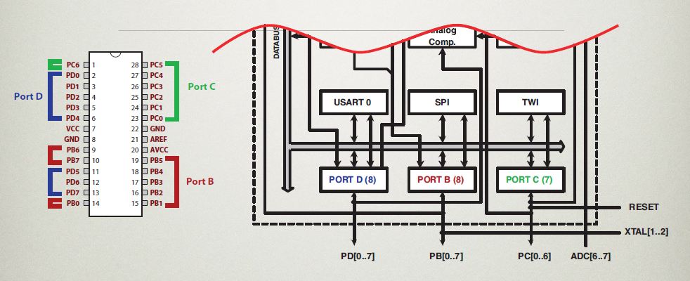
GPIO PORTS
- Three 8-bit IO ports
- Port-B, Port-C & Port-D
- pins identified as PBx, PCx and PDx where x=0...7
- Each pin can be configured as:
- input with internal pull-up
- input with no pull-up (Hi-Z configuration)
- Output low
- Output high
Alternate Port Functions

- Most port pin have alternate functions
- Internal peripherals use the alternate functions
- Each port pin can be assigned only one function at a time
Timers/Counters
- 8/16 bit register
- increment or decrement on every clock cycle
- can be read on data bus
- output feeds waveform generator
- Clock sources
- Inter from clock prescalar
- External Tn Pin
- Multiple operating modes
- simple timer/counter
- output compare function
- waveform generator
- Clear/set/toggle on match
- frequency control
- PWM


n can be 0,1, and 2.
Controlling the frequency:
Here, the duty cycle is constant while frequency is being changed.

PWM:

Here, frequency is constant while duty cycle is being changed.
FAST PWM MODE:
- Counter counts from the BOTTOM(0) to MAX possible value.
- Counter reset to 0 at MAX
- OCnx cleared at TOP
- OCnx sets at BOTTOM

ADC:
- 10bit successive approximation ADC
- 8 channel multiplexer using port pins ADC0-7: multiplexer is used to select the one channel at a time need to be converted.
- Max conversion time 260 usec
Analog Comparator:
- Compares voltages between pins AIN0 and AIN1
- Asserts AC0 when AIN0 > AIN1
- AC0 can trigger timer capture function
- Range finders indicate distance with pulse width
- Timer capture mode can compute pulse width
SPI(Serial Peripheral Interface):
- Industry standard serial protocol for communication between local devices
- Master/slave protocol
- 3-Wire interface
- Slaves addressed via slave select(SS) inputs

I2C BUS Interface:
- Industry standard serial protocol for communication between local devices
- Master/slave protocol
- 2-Wire interface (TWI)
- Byte oriented messages
- Slave address embedded in command


USART:
- Universal synchronous and asynchronous Receiver and transmitter
- Full Duplex operation
- High resolution baud rate generator
- Can provide serial terminal interface
L7....................
GPIO:
All the GPIO pins have true read-modify-write ability
the direction of one port pin can be changed independently of the other pins
PORT: x
PIN: n

Circuit diagram for each pin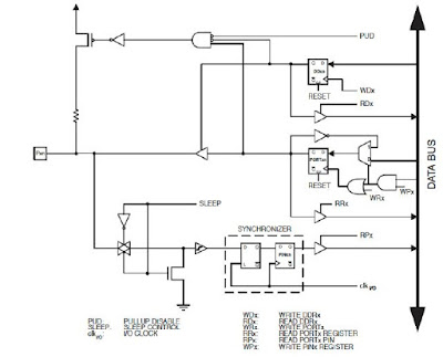
Arduino Ports:

Now, we will be talking about the necessary registers used to control the GPIOs and those registers are
- PORTx: controls the value of the pins
- DDRx: controls the direction of the pins(I/O)
- PINx: reads the value of the pins
where, x can be B,C or D. These registers are associated with each port
Each pin can be configured as Input state, Output state and Alternate function

Tri-state (Hi-Z) is the true input state, when we want to use a pin as input then we put the put in Tri-state. Meaning:
INPUT: Tri-state(Hi-Z)
INPUT_PULLUP: Pxn will source current is ext. pulled
whenever we write 1 to the direction register to make the pin as output pin then the pull up register is disabled, meaning in Atmega328 we cannot use the internal pull up register in case the pin is configured as output pin.
Let say we want to change the direction of the pin from input to output or from output to input then we can do this but with some restrictions: like we cannot change the DDRx register and PORTx register at the same time(We can make these transition by changing a bit at a time and then change the another bit after inserting a delay between these two transitions). So one must remember, what transition we can make and what we cannot while programming.
Now, let see the port-B register closely

The reddish color indicates that the words are predefined in Arduino IDE. And hence, we can use PORTB7 and PINB7 but cannot use DDRB6 in Arduino IDE.
Default values for PINB register is not defined.
Port-C register:

Port D register:

It is important to note that all the pins are configured as input(Tri-state(hi-z)), this is because the DDRx has 0 as default value.
Steps to write to a pin on a port:
- prepare the pin to be an output pin(as required): DDRx_Bitn
- Write the data to the pin: Portx_Bitn
Ways of setting pins:
- Directly: DDRC = 0b01101100;
- Bit shifting: PORTB = (1<<2)|(1<<3)|(1<<5)|(1<<6);
- OR-ing with a mask (specific bits, leaving the rest as it was: DDRD |= 0b00010100;//setting bits 2 and 4 or DDRD |= ((1<<2)|(1<<4));
Ways of clearing pins:
- Directly: DDRC = 0b01101100;//clearing 0,1,4,7th bits
- AND-ing with a mask(specific bits, leaving the rest as it was): DDRD &= 0b11101011; //clearing bits 2 and 4, DDRD &= ~((1<<2)|(1<<4));
Checking a Pin-State:
- AND with a mask: PINB & 0b00010000;//checking the pin-4 state
Toggling a Pin state:
- Even though PINx is for reading a port, if you write a 1 to any pin, it will toggle that pin
- The pin in PINx are supposedly the read-only
- Writing a 1 to pin doesnt set the pin, toggles it.
- Writing a 0 to a pin deosnt clear it, it leaves it unchanged.
- PINB = (1<<5);//toggles only pin-5
Programming example:
- in the setup function, set up
- the forst 3 digital PWM pins as output
- the Rx as input
- the Tx as output
- The remainder of the first 8 Arduino pins as input
- in the loop function
- read the input pins
- set the corresponding output pins as the NOT of the inputs
Understanding the problem:
- Meaning we are only talking about the PORT-D
- the PWM pins among these are pins 3, 5, and 6
- the Rx and Tx pins are 0 and 1
- we assign (0,2,4,7) as input pin and corresponding (1,3,5,6) as output pins respectively.
Solution
void setup(){
DDRD=0b01101010;
PORTD |=0b11111111;//sets all the bits to 1. Meaning all the pins configured as input //will get their pull-up resistor enabled, so its not a good //practice to write 1 to all the pins. It might not be the problem //for this perticular question but doing so can be problematic in //other conditions. Instead write: PORTD|=0b01101010
}
- |= takes whatever in the PORTD and or it with the 0b11111111 and then write back the result into the PORTD register
- Question: what happens if a bit is written to that has been set as an input pin. Meaning we have first configured a pin as input and we are writing 1 to it. Answer: If we have set a pin as input and writing 1 to it then the pull-up resistor to that pin will be activated.
void loop(){
if(PIND0 == 0) PORTD |= 0x02; //set the pin-1 and don't effect the others
if(PIND0 == 1) PORTD &= 0xFD;//reset pin-1 and don't effect the others
if(PIND2 == 0) PORTD |= 0b00001000;//set pin-3 " " "
if(PIND2 == 1) PORTD &= 0b11110111;//reset-3 " " "
if(PIND4 == 0) PORTD |= 0b00100000;//set-5 " " "
if(PIND4 == 1) PORTD &= 0b11011111;//reset-5 " " "
if(PIND7 == 0) PORTD |= 0b01000000;//set-6 " " "
if(PIND7 == 1) PORTD &= 0b10111111;//reset-6 " " "
}
- PORTD |= 0b01000000;
- PORTD &= 0b10111111;
- These two above lines are equivalent of writing the pin-6 using digitalWrite(pin-6, HIGH)
and
- if(PIND7==0)
- if(PIND7==1)
- These two above lines are equivalent to digitalRead(pin-7)
Synchronization when reading an externally applied pin value: Synchronization when reading a software assigned pin value:
 Alternate Function Port:


PORTB pins alternate function:


GPIO as output:
- When a pin is set as output then it is in low-Z state, and it can source current at max 40mA
- Shorts or attempting to draw more current can fry the arduino
- use external resistors to limit current from the pins
- Pin13 on Arduino uno board has a LED pull-up resistor connected.
GPIO as input:
- All pins can be used as digital inputs, by default a pin is configured as input, and the pin configured as input are in high-Z state, and in this state they draw a very little current and don't load the circuit they are attached to.
- If the pin is not connected to a circuit, then the pin in high-Z state will be in floating state and read unpredictable values, this unpredictable values are because of the capacitive coupling with the neighboring pin.
- Unconnected inputs consume more power than inputs that are pulled up or low through resistor.
Micro-Controller Control Register:

BOD(brown out detect)
Comments
Post a Comment