EH#4: Understanding the LPDDR4 SDRAM memory for mobile, automotive and embedded system applications.
- Get link
- X
- Other Apps
In order to better understand the RAM, we will take an example of MT53D512M16D1DS-046 from Micron and will see what all should be known to use this RAM for any project.
Introduction
Micron's MT53D512M16D1DS-046 is a high-performance LPDDR4 DRAM chip that brings impressive speed and power efficiency to mobile, automotive, and embedded applications. In this blog, we will explore the chip's technical specifications, internal architecture, and key terms such as die count, rank, and memory organization. Whether you're a hardware engineer or an enthusiast curious about modern memory design, this breakdown will guide you through everything you need to know.
- The Mobile Low-Power DDR4 SDRAM (LPDDR4) is a high-speed CMOS, dynamic random-access memory internally configured with either 1 or 2 channels. Each channel is comprised of 16 DQs and 8 banks.
- LPDDR4 uses a 2-tick, single-data-rate (SDR) protocol on the CA bus to reduce the number of input signals in the system. The term "2-tick" means that the command/address is decoded across two transactions, such that half of the command/address is captured with each of two consecutive rising edges of CK. The 6-bit CA bus contains command, address, and bank information. Some commands such as READ, WRITE, MASKED WRITE, and ACTIVATE require two consecutive 2-tick SDR commands to complete the instruction.
- LPDDR4 uses a double-data-rate (DDR) protocol on the DQ bus to achieve high-speed operation. The DDR interface transfers two data bits to each DQ lane in one clock cycle and is matched to a 16n- prefetch DRAM architecture. A write/read access consists of a single 16n-bit-wide data transfer to/from the DRAM core and 16 corresponding n-bitwide data transfers at the I/O pins.
Overview and Key Specs
The MT53D512M16D1DS-046 is an LPDDR4 SDRAM device with the following headline specs:
- Memory Density: 8 Gbit (8,192 Mbits), organized as 512 million words of 16 bits each (512M × 16 bits)
- Data Rate: Up to 4266 MT/s (2133 MHz clock)
- I/O Voltage (VDDQ): ~0.6V, optimized for low power applications
- Core Voltage (VDD): 1.06V to 1.17V, with a typical value of 1.1V
- Bus Width: 16 bits
- Package Type: 200-ball Wafer-Level Chip-Scale Package (WFBGA), compact 10 × 14.5 mm footprint
- Operating Temperature Range: -40°C to +95°C (standard), up to +105°C for automotive AAT grade
- Target Applications: Mobile devices, automotive systems, and industrial electronics
Typical Applications
Micron’s MT53D512M16D1DS-046 can be found in:
- Smartphones and tablets
- In-vehicle infotainment (IVI) and driver assistance systems
- Embedded systems in industrial control units
- Wearables and ultra-compact computing platforms
understanding rank, die count, and memory organization
when working with DRAM like LPDDR4. Let’s break these terms down clearly using the Micron MT53D512M16D1DS-046 as an example.
Die Count
- A die is a single piece of silicon inside a chip.
- Some memory chips contain multiple dies internally (multi-die packages).
- The MT53D512M16D1DS has 1 die (as per specs). So all the memory is built into a single silicon die.
Memory Organization
- Memory chips are structured by:
- Density: The total capacity — here it’s 8 Gbit (gigabits)
- Organization: For this chip, it's 512M × 16
- This means: 512 million memory locations, each 16 bits wide
- 16-bit bus width = data is accessed 16 bits at a time
- So this device provides 8Gbit of memory organized as 512M words, each 16 bits.
Rank
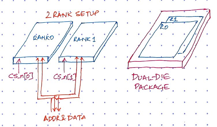
- A rank is a group of memory chips (or a portion of a chip) that responds to the same chip select (CS) signal and can be accessed simultaneously.
- A single-rank memory device has one group of memory that’s active at a time.
- A dual-rank device acts like two banks of memory inside one module — useful for performance (interleaving), but more complex.
In LPDDR4, a "rank" often corresponds to a die. Since this device has 1 die, it's single-rank.
Package Block Diagram:
Power-up sequence: VDD1 must ramp at the same time or earlier than VDD2. VDD2 must ramp at the same time or earlier than VDDQ. For device durability, please follow the proper power-off sequence as well, refer to the datasheet.
- DataGroup (Data bits: DQ, Data strobe: DQS, Data Mask: DM, Check bits)
- Address and Command Group (CA)
- Control group (Chip Select: CS, Clock enable: CE, on die termination:ODT)
- Clock group (clock signals: CK)
Further Reading...
- https://www.systemverilog.io/design/ddr4-basics/#
- Get link
- X
- Other Apps


Comments
Post a Comment